Meet the ZedRipper – a 16-core, 83 MHz Z80 powerhouse as portable as it is impractical. The ZedRipper is my latest attempt to build a fun ‘project’ machine, with a couple of goals in mind:
- Finally use one of the giant FPGA boards I had lying around
- Play a little ‘alternate-history computer engineering’ with a hardware-focused approach to multitasking
- Build a machine that I could write fun, small programs for on my daily train ride
- Build a platform that would allow for relatively easy computer-architecture experiments
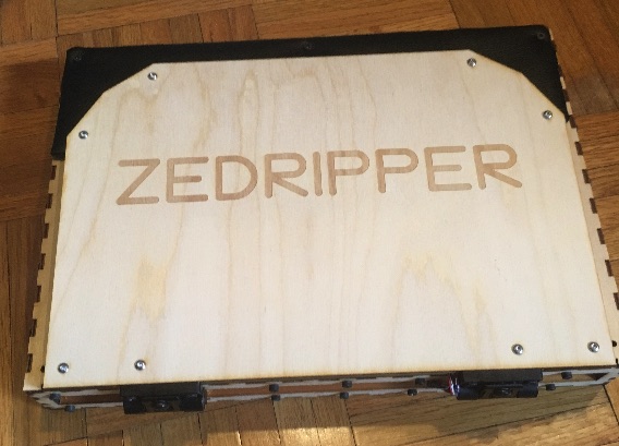
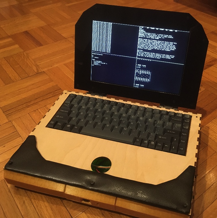
Glamour Shots
For those that don’t have time for a wall of text about impractical computer architecture…
What is this beast?
The ZedRipper is basically my attempt to build the ultimate CP/M 2.2 computer.
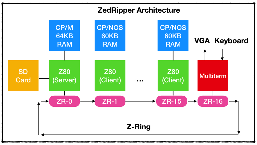
- 16-core Z80 processor running at 83.33 MHz
- 64KB of dedicated RAM for each Z80
- 16-way ANSI-compatible “Multiterm” terminal accelerator
- All CPUs and devices connected with a fully-synchronous, uni-directional ring network operating at 83 MHz
- 128MB of storage on SD Card (available via 16 x 8MB disk drives in CP/M)
- A ‘server’ core that boots into CP/M 2.2 and runs a CP/NET file server (written in Turbo Pascal 3 on the machine!) allowing shared access to the SD card
- 15 ‘client’ cores running CP/NOS from ROM. Each client can access the shared storage and run any CP/M 2.2 programs without resource contention with the other cores.
The Road Not Taken
My adventures with porting a game to my Kaypro left me with surprisingly warm feelings towards this primitive, 40 year old operating system, and I had an idea that I wanted to explore – what if history had taken a different turn, and personal computers had gone down the multi-CPU path right from the start? Even in the 1980s the CPUs themselves (and pretty quickly, the RAM, too) were fairly cheap, but multi-tasking for personal computers was exclusively focused on a ‘time-slicing’ approach whereby one big resource (the RAM or the CPU) got split between competing programs. The hardware just wasn’t really up to the task (and it was extremely difficult to make programs for OSes like DOS play nicely with one another) until we got well into the 386-era and computers with 4MB+ of RAM.
In the course of my historical computing hobbies, I stumbled upon something that I thought was very fascinating – relatively early in its history, CP/M supported a ‘networked’ version called CP/NET. The idea behind it was was one that will still feel pretty familiar to most people – that an office might have one or two ‘real’ machines with large disk drives and printers that it shared with ‘thin-client’ style machines that we’re basically just terminals with CPUs and RAM attached. Each user could basically act as if they had their own private CP/M machine with access to large disks and printers.
As I mentioned, the CPU and RAM (typically a Z80 with 64KB of DRAM) weren’t terribly expensive, but all of the trappings required to make something a useful computer (disks, printers, monitors, etc.) really added up. Adding additional CPU(s)+RAM somehow just felt too decadent at the time for someone to consider providing a single user with multiple CPUs and RAM. Even CP/M went the time-sliced multi-tasking route with the MP/M OS.
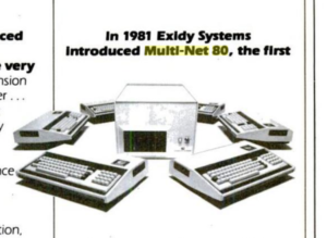
I found a company called Exidy that came the closest – in 1981 they released their “Multi-NET 80” machine, which allowed up to 16 Z80+RAM cards to be added to it, but it was once again designed to serve 16 individual users rather than a power user with 16 simultaneously running programs.
Fast-forward 40 years, and transistors are very cheap indeed. I inherited some pretty monster FPGA boards (Stratix IV 530GX parts) following a lab cleanup, and was looking for something fun to do with one of them. I had stumbled upon Grant Searle’s extremely fun “Multi-Comp” project at some point, and it was pretty easy to get a single-CPU CP/M machine up and running. But I wanted more. I had 530,000 LUTs and megabytes of on-die block ram just waiting for a cool idea. I decided to go big and see if I could build my own multi-core CP/M machine with true-multitasking – nothing clever, just brute force.
Getting the software up and running
I took a pretty hardware-centric approach to this project, and I didn’t actually write a single line of assembly. CPU 0 boots straight from the ROM Grant provided for his multi-comp project, and the other nodes actually boot from a 4KB CP/NOS ROM I found from an Altair simulator.
Both ROMs expect to interface with a serial terminal with a pretty standard interface, and the CP/NOS clients expect another serial port connected to a server. As custom logic is basically free on such a large FPGA, I designed some custom address-decoding logic that makes each CPU’s Z-Ring interface appear where it’s expected in the I/O address map.
The Internals
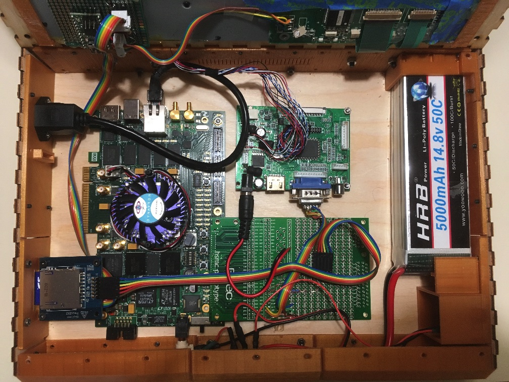
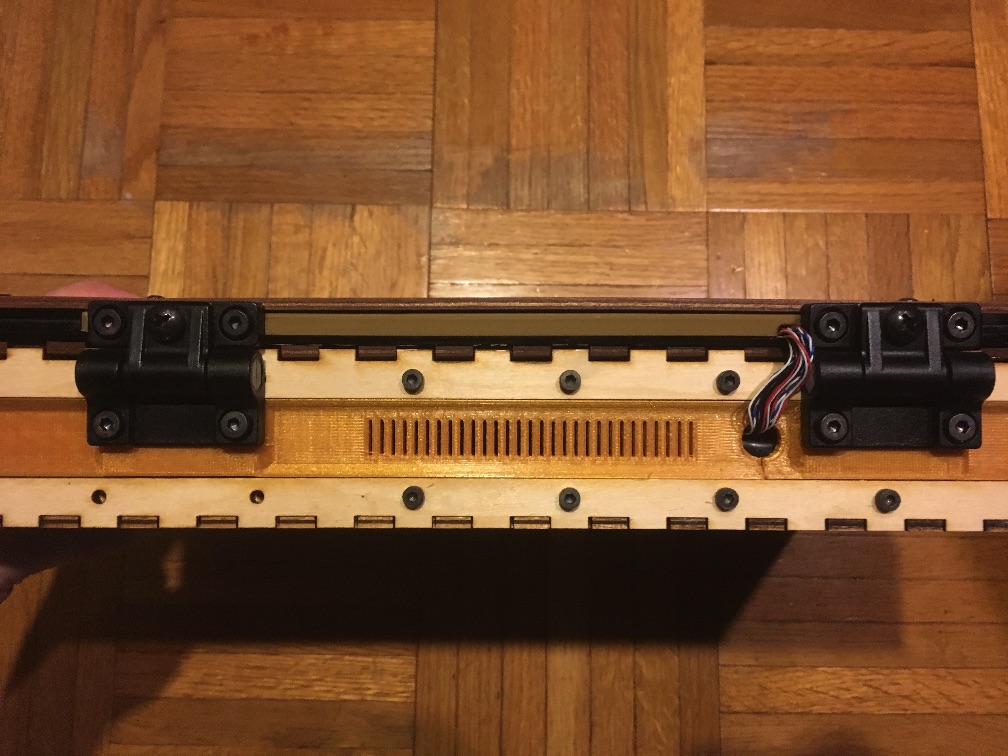
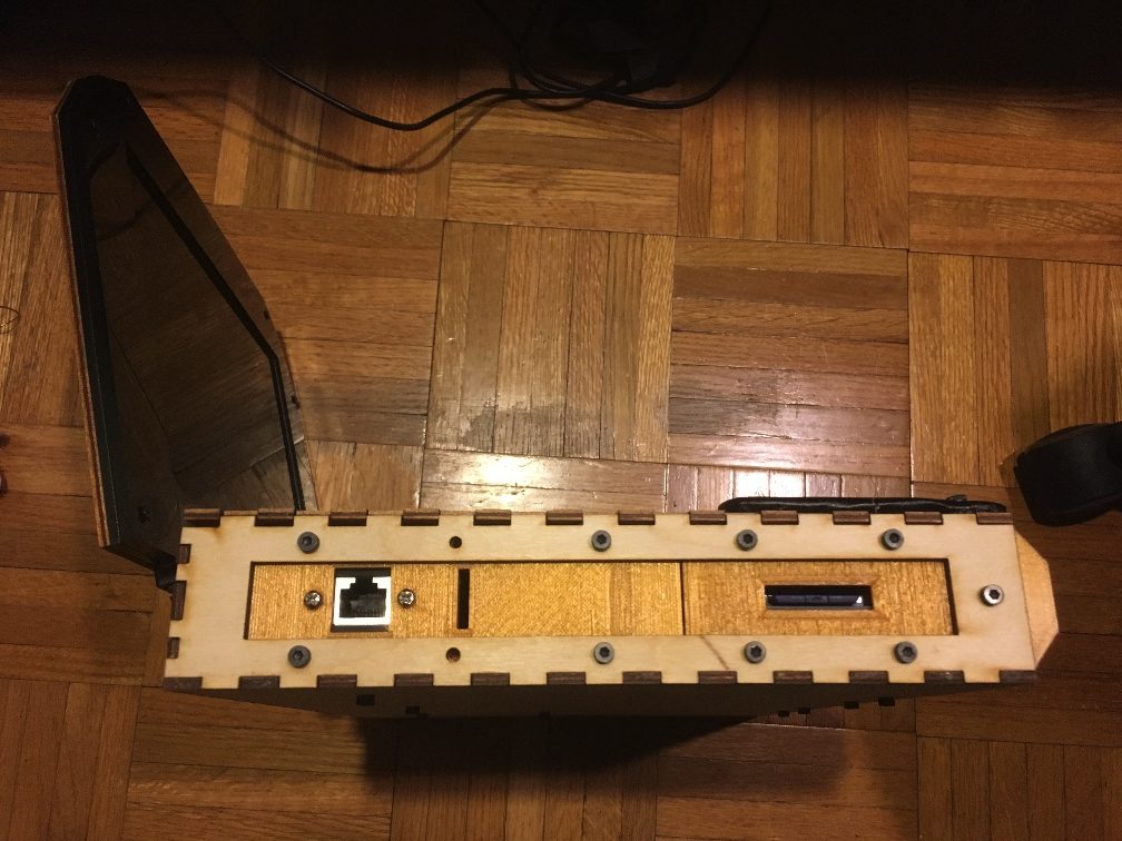
The heart of the ZedRipper is one of these monsters sporting a Stratix IV 530GX FPGA. An HSMC breakout card is used to drive the display, receive data from the keyboard controller and connect to the SD Card. You actually use ethernet to upload a new firmware image, so the ethernet port is routed to the side of the case, along with the SD Card adapter and a (currently unused) slot for an external serial port.
The Keyboard and Controller
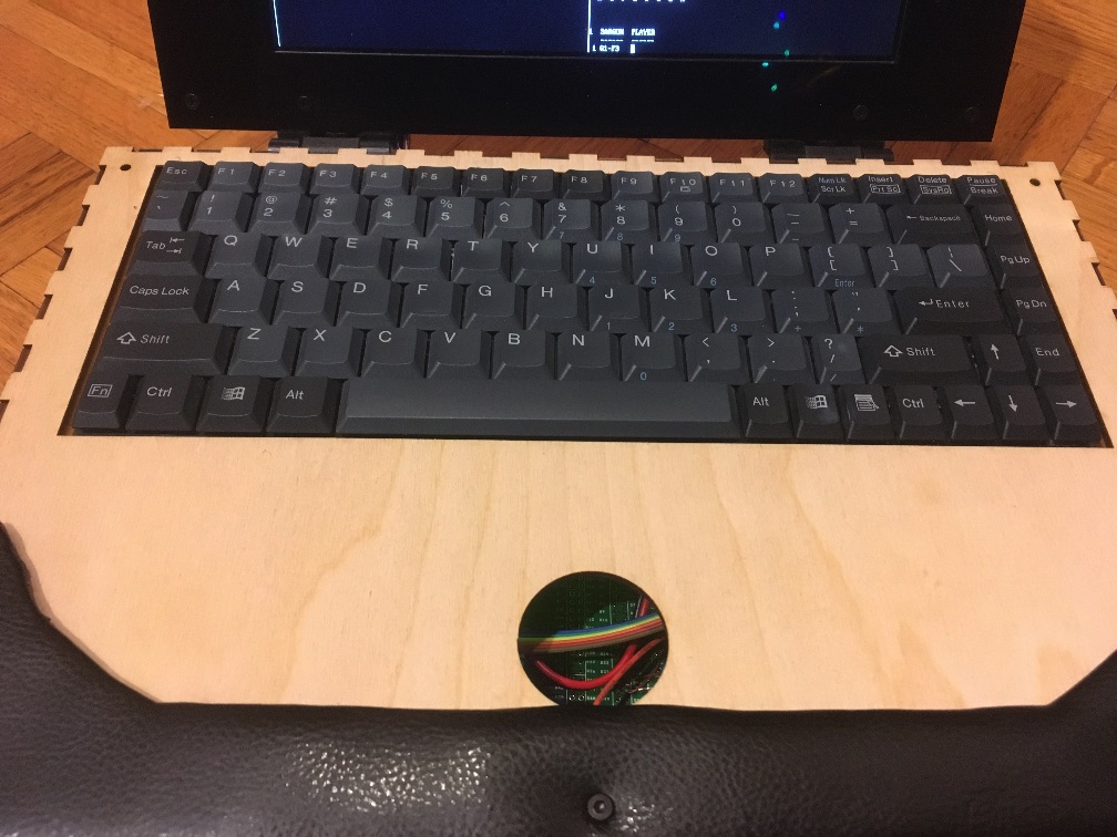
I had a compact PS/2 keyboard lying around (salvaged from one of my old laptop projects, actually) that I wanted to interface with the 2.5V I/O on my FPGA. I decided to go the ‘easy’ route, and toss in a Teensy 2.0 microcontroller.
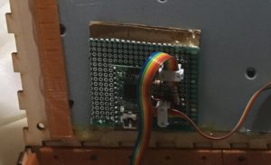
This does the PS/2-to-ASCII translation, and also allows easy mapping of some of the weirder keys (like F1-F12) to ‘magic’ terminal sequences for convenience. The Teensy then outputs bytes to the Z80 over a 9600 baud UART (with a simple resistor voltage divider to change the 5V output into 2.5V for the FPGA). Given that this whole project is basically cobbled together from things lying around my workshop, this was a convenient solution that worked out quite well.
The Display
The display is a 1280×800 10.1″ display that accepts VGA input. The FPGA uses a simple resistor network to generate up to 64 colors (R2G2B2). The screen requires an 83.33 MHz pixel clock (1280×800@60Hz), so for simplicity’s sake, the entire design runs synchronously at that frequency.
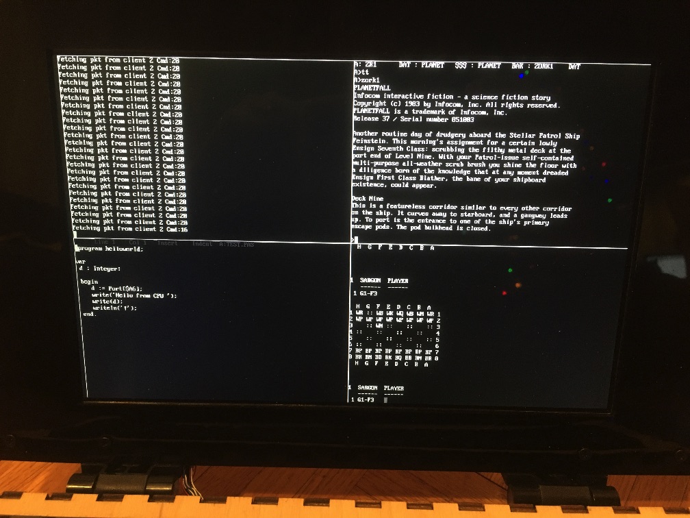
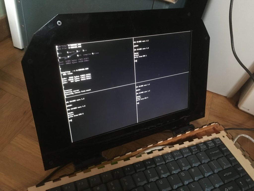
Grant’s Multicomp project included VHDL code for a basic ANSI-compatible terminal. I re-wrote the terminal logic in Verilog (just for my own sanity), and then designed a video controller that supports 16 fully independent terminals, all connected via a single Z-Ring node. The 1280×800 display is effectively treated as a 160×50 character-based display (using an 8×16 font), and each terminal acts like an 80×25 ‘sprite’ that can be re-positioned anywhere on the screen (with a priority list to configure the order of precedence for the terminals being drawn). As each terminal is fully independent, it contains its own state machine, along with a 2KB character RAM and 2KB ‘attribute’ RAM (to hold the color information). Each character supports a 4-bit foreground and background color. Since all of the terminals must maintain the same character alignment, any given 8×16 ‘cell’ on the screen can only contain a single character, and all 16 terminals can share a 2KB ROM containing the font. In total then, the display logic uses up around 66KB of Block RAM.
The general effect of this is that I have an extremely simple window manager for my CP/M terminals, almost entirely in hardware. This is one of the areas that’s most fertile for exploring – at the moment only the server CPU is capable of re-positioning the terminals, but I have longer term plans to add in a mouse-like positioning device to allow a hardware-only mechanism for dragging windows around and changing the display priority.
As the terminal controller is just another node on the Z-Ring (and the Z-Ring interface for each Z80 is straightforward to re-target), future plans include possibly adding a ‘full-screen’ 160×50 terminal (possibly as a ‘background’) and an actual 1280x800x64-color bitmapped display using some of the fast external SRAM on the board.
The Z-Ring
Conjuring a pile of Z80s into existence is as easy as writing a generate loop in verilog, but how to connect them up in a sane way? One thing I’ve learned from my day job is that designing a network can be hard. General goals for this network:
- Simple implementation
- Simple Interface
- Arbitrarily expandable
- Adequate Performance
As I mentioned earlier, my Z80s were expecting to interface with some serial ports, so the interface was fairly simple – make it look like a serial port! At its core, the Z-Ring is a synchronous, uni-directional ring network that uses credits for flow control. Each node contains a 1-byte receive buffer for every other node on the network. Coming out of reset then, each node has 1 ‘credit’ for every other node on the network. The design is parameterized, so it could easily scale up to hundreds of nodes with only a bit more logic, but as it’s currently implemented the Z-Ring supports up to 32 nodes (so each node requires a 32-byte buffer).
The actual ‘bus’ consists of a valid bit, a ‘source’ ID, a ‘destination’ ID and a 1-byte payload (so 19 bits wide). I think it would be pretty straightforward to implement this using TTL logic (if one found themselves transported back to 1981 and couldn’t use FPGAs). Each ‘node’ has 2 pipelined sets of flops on the bus – stage 0 and stage 1 – and when you inject a message, it waits until stage 0 is empty before muxing it into stage 1. Messages are injected at the ‘source’ node and travel around the ring until they reach their destination node, at which point they land in the corresponding buffer and update a ‘data ready’ flag. When the receiving node reads from the buffer, it ‘re-injects’ the original message which continues around the ring until it reaches the source again, thus returning the credit. A ‘feature’ of this scheme is that if you do send a packet to non-existent address, the credit will be automatically returned to you when it loops back around.
As each stop on the ring consists of 2 pipeline stages, and there is no backpressuring, each message takes no more than 2*(number of nodes) cycles to be delivered. The current implementation has 17 nodes (16 CPUs + the display/keyboard controller) and runs with a 12nS clock, so to deliver a message and receive the credit back you are looking at a minimum of ~400 nS. The display controller can basically sink traffic as quickly as it arrives, so each CPU has ~2-2.5 MB/s of bandwidth to its own terminal (with enough shared bandwidth on the bus to accommodate all 16 CPUs), which is quite a bit as far as terminals go.
The current implementation is perfectly adequate to get things up and running, but there are a number of pretty straightforward improvements that could be made:
- Adding deeper receive buffers would potentially allow much higher bandwidth from a given node – there are plenty of free 1KB block rams on the FPGA, which would allow 32 credits x 32 nodes, so each CPU would in theory be capable of saturating the bus.
- Add support for an ‘address’ mode – Adding a 16-bit (or more!) address would allow DMA operations between nodes (and adding a simple DMA engine to each node would be pretty easy). The FPGA board has a ton of extra hardware (several megabytes of varying static RAMs, and a gigabyte or so of DDR3) that could be potentially fun to interface with.
- Add some sort of flow-control (and buffering) between nodes to allow more flexible decoupling.
But I’m perfectly content to leave those for a future rainy day for now.
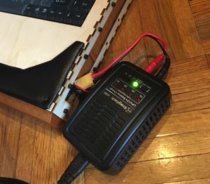
Power!
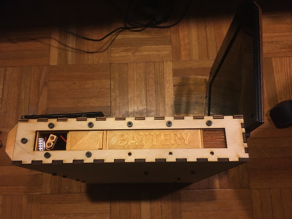
The FPGA dev board requires a 14V-20V input, while the display requires a 12V input, and the Teensy and PS/2 keyboard requires a 5V input. Conveniently, the FPGA board has 3.3V, 5V and 12V regulators that are relatively easy to tap into, so the FPGA board accepts power directly from a beefy 5000 mAh / 14.4V LiPo battery pack and then supplies power to all of the other devices. One of the trickier bits of this project was that I didn’t want to have to dis-assemble the laptop to re-charge it, but the battery has both the normal +/- power connector, as well as a ‘balance’ connector that connects to each individual cell for recharging purposes. My somewhat ‘meh’ solution to this was to have the power switch toggle between connecting the main supply to the FPGA and to a charging plug (along with the balance connector) in a little internal compartment exposed by a sliding door. It’s kind of awkward, but you can just slide the door open and fish out the connectors to plug into the charger without needing to break out an M3 hex key.
I haven’t actually tested it properly, but the battery lasts for 3+ hours (which is more than adequate to cover my daily train ride). If I had to guess it’s probably closer to the ~6 hour range without any power optimization effort on my part. It doesn’t support simultaneous charging / usage, but the battery life is sufficiently good that it hasn’t been a problem.
The Case
The case is fairly standard ‘hackerspace’ construction – a combination of laser-cut 3mm plywood and 3D printed plastic for everything else. I sprung for proper position-control hinges for the screen, so it feels like a relatively normal (if somewhat less svelte) laptop when you’re using it. I wanted to give it some 1980’s flair, so the screen actually has some “Cray”-ish angles at the top, and there is a pleather wrist-rest. The actual edge of the laser-cut plywood is pretty uncomfortable against your wrists while typing, so the wrist-rest is surprisingly functional.
Benchmarking!
I haven’t tried any actual CP/M benchmarking programs (I assume there are some out there, but I’ve never looked very hard), but, as this machine was mostly built with writing Turbo Pascal in mind, I did at least try some micro benchmarks. I can do between 15k-35k floating point operations/sec (using the 48-bit Real type in TP), and ~1 million integer operations/sec (using the 16-bit Integer type in TP), so all-in-all not too bad for an 8-bit CPU and a fairly nice programming environment.
Designing a floating point accelerator might be a fun project some day, and there is plenty of logic resources to support it.
FPGA Utilization
As I’ve mentioned before, all of the logic so far is pretty lightweight, occupying a mere 7% of on-chip logic resources (although ~40% of the total on-chip block ram and 100% of the big M144k block rams).
Combinational ALUTs 31,808 / 424,960 ( 7 % )
Memory ALUTs 0 / 212,480 ( 0 % )
Dedicated logic registers 10,231 / 424,960 ( 2 % )
Logic utilization 10 %
Total registers 10231
Total block memory bits 9,005,056 / 21,233,664 ( 42 % )
DSP block 18-bit elements 0 / 1,024 ( 0 % )
There is plenty of room for fun experimentation going forward (and remarkably, compiling this project only takes ~10 minutes).
Future Plans
I have immediate plans (as in, I have the hardware lying around, I just haven’t had time to solder it yet) for the following:
- Stain and seal things! It’s made of thin plywood. It really wants to be coated in something.
- Joystick-like pointing device – to be connected to the Teensy that acts as a keyboard controller and fill that conspicuous hole.
- Battery Monitoring – once again, the ADC on the Teensy is going to provide some lightweight battery monitoring so that I have some idea how charged things are
- WiFi – I have an ESP32 lying around waiting to run Zimodem! Coupled with my phone in wifi hotspot mode, it should allow me to have ‘net access on the go =) There are good terminal apps available for CP/M, but it would be fun to try to write things like an IRC client or a very simple web browser. It also allows convenient use of kermit for file transfers to a modern computer running linux.
- Add an externally-accessible serial port for communicating with another machine (there is already a 3D-printed slot for the connector, I just need to wire it in)
- Status LED! There’s already a mounting hole in the front – current plan is to connect it to the SD Card’s drive access signal.
Longer term, there are lots of neat hardware ideas that might be fun to experiment with:
- How fast can you make a Z80 go? The first step would be to decouple the CPU speed from the pixel clock, but it would also be fun to try applying some modern computer architecture techniques to a Z80 (pipelining, register re-naming, branch prediction, wider memory for pre-fetching, etc.)
- Similarly, adding custom accelerators for things like floating point might be fun. There are 1024 completely unused DSP blocks on this chip, and I bet no one has tried to build an accelerator for the 48-bit Real format that turbo pascal uses.
- Use the existing hardware! This development board is brimming with unused memory, primarily:
- 512 MB DDR3 SDRAM with a 64 bit data bus
- 128 MB DDR3 SDRAM with a 16 bit data bus
- Two 4 MB QDR II+ SRAMs with 18 bit data buses
- 64 MB flash
- 2 MB SSRAM
- Better video hardware! The first step would probably be to add support for a ‘full-screen’ 160×50 terminal and the ability to scale a regular 80×25 terminal up by 2x. The aforementioned external SSRAM would also make it quite straightforward to add a full 1280×800@6-bit, fully bit-mapped display.
- Expand the capabilities of the current terminal – I think I could add compatibility with the ADM-3A-ish terminal (plus graphics support) used by the Kaypro/84 series, so that way I would have access to a slightly larger set of software (and not have to port DD9!). I could also probably think of custom escape sequences that might be convenient to add.
Final Thoughts
I’ve only had the machine up and running for a few days, but I’ve got to say, it’s pretty great. The screen is nice and clear, the keyboard is spacious and comfortable, and it’s bulky, but it doesn’t actually weigh all that much (and still easily fits in my backpack). It’s even surprisingly ergonomic to use on the train.
Usage-wise, I also think I’m really on to something. Just the ability to have a text editor open for taking notes in one window while I’m debugging some turbo pascal code in another window is extremely convenient (or taking notes while playing Zork!). It feels like this could have been a genuinely viable approach towards building a low-cost, multi-tasking CP/M environment.
Itching to build your own?
I don’t actually have an easy way to get files *off* of the machine yet, so for now the most useful part (the CP/Net file server written in Turbo Pascal) is kind of trapped on the machine. Stay tuned for a future update with all of the Verilog and TP code though (and shoot me an e-mail if you really can’t wait). At some point I should probably join the 21st century and get a github account, too. Alas, that whole ‘free time’ thing…